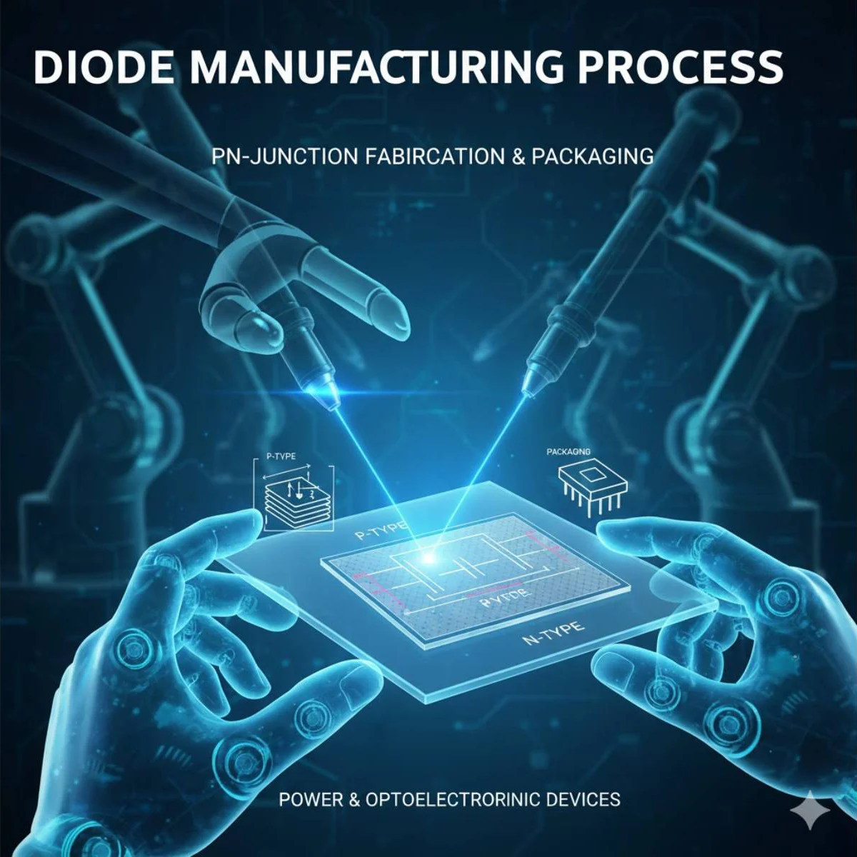
Diode Manufacturing Process
Diodes are fundamental components in power semiconductors and analog devices, widely used for rectification, protection, switching, and signal control. The core of diode manufacturing lies in precisely defining multiple device layers, junction regions, and metal electrodes on silicon wafers. M&R focuses on photolithography process equipment, supporting process engineers in both R&D and mass production by maintaining stable critical dimension control, alignment accuracy, and process repeatability to ensure consistent electrical performance and device reliability.
Diode manufacturing involves several core process steps, including diffusion, ion implantation, thin-film deposition, metal contact formation, and final packaging. Depending on the application, the process is differentiated for power diodes, photodiodes, or Schottky diodes. For example, power diodes require high breakdown voltage and low on-resistance, demanding strict control over chip structure and defect density. Photodiodes emphasize response speed and sensitivity, making them suitable for fiber-optic communications and sensing applications. With the rapid growth of 5G, AI computing, and new energy vehicles, diode processes face increasing challenges in current density and thermal management. Achieving an optimal balance between reliability, efficiency, and cost remains a key focus of ongoing process optimization.
Key Challenges in Display Panel Manufacturing
Diode fabrication requires precise control of P–N junction locations, junction depths, and electrode structures within limited device dimensions. As device miniaturization and power density continue to increase, higher demands are placed on photoresist coating uniformity, exposure critical dimension control, and alignment accuracy. Even minor process variations can result in increased leakage current, shifts in breakdown voltage, or yield loss, making equipment stability and repeatability critical factors for successful diode production.
The Role of Photolithography Equipment in Display Manufacturing
Photolithography equipment plays a key role in diode manufacturing by defining diffusion regions, guard rings, metal contacts, and termination structures. Stable exposure energy, precise critical dimension control, and reliable alignment performance are essential to ensure accurate downstream processes such as ion implantation, diffusion, and metallization. These capabilities directly impact the diode’s electrical characteristics, voltage endurance, and long-term reliability.
Process Requirement Differences Among Display Technologies
Different diode types place varying emphasis on photolithography process capabilities.
Standard rectifier diodes focus on junction uniformity and high-volume manufacturing stability;
Schottky diodes require precise control of metal–semiconductor contact regions and line widths to achieve low forward voltage;
while power diodes and fast-recovery diodes demand higher standards in guard ring definition, alignment accuracy, and defect control. As a result, photolithography equipment stability and repeatability become key enablers for process qualification and mass production.
M&R Technology’s Equipment Support for Display Panel Manufacturing
To meet the requirements of diode manufacturing, M&R provides photolithography process equipment solutions covering coating, exposure, development, cleaning, and integrated front-end processes. These solutions help process engineers maintain stable pattern transfer quality and alignment accuracy across various device sizes and process conditions. With flexible equipment configurations and comprehensive process support, M&R effectively supports diode manufacturing from R&D validation through process optimization and high-volume production.
Application Industries
Diode manufacturing processes are widely applied across power management, automotive electronics, industrial control, consumer electronics, renewable energy, and communication equipment industries. These applications demand high reliability, voltage endurance, and consistent mass production quality, making stable and repeatable photolithography equipment a critical foundation for successful diode manufacturing.