MEMS manufacturing processes
Micro-Electro-Mechanical Systems (MEMS) manufacturing integrates semiconductor processing with micromechanical structure technologies and is widely applied to sensors, actuators, and microsystems. The core objective is to achieve stable and repeatable multilayer material deposition, microstructure pattern definition, deep etching, and precise alignment within a high-cleanliness environment, enabling the integration of electrical, mechanical, and structural functionalities in miniature devices.
M&R Technology focuses on photolithography-related equipment for semiconductor manufacturing, supporting MEMS process engineers during both R&D introduction and mass production by maintaining microstructure dimensional control, alignment accuracy, and overall process consistency to ensure device performance and reliability.
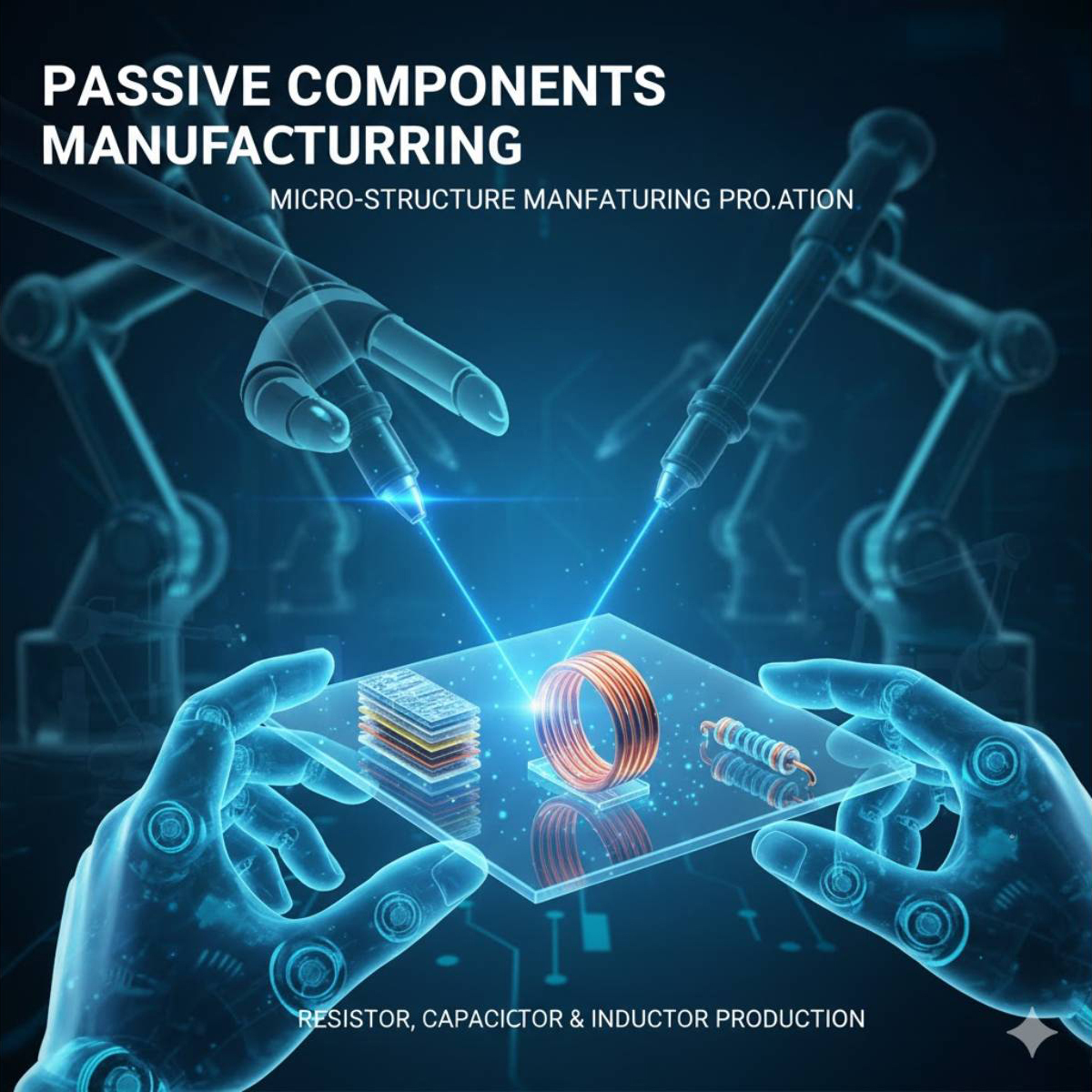
Microelectromechanical systems (MEMS) manufacturing combines semiconductor fabrication with mechanical processing technologies and is primarily used for sensors, actuators, filters, and medical chips. Common process steps include silicon-based etching, thin-film deposition, microstructure fabrication, and back-end packaging. Compared with conventional IC processes, MEMS places greater emphasis on three-dimensional structural design and release steps, requiring careful management of surface tension effects and structural warpage during manufacturing. MEMS applications are wide-ranging, including accelerometers and gyroscopes in smartphones, radar sensors in autonomous vehicles, and pressure-sensing chips in medical devices. With the growing adoption of the Internet of Things (IoT) and automotive electronics, MEMS processes face increasingly stringent requirements for stability, mass-production yield, and cost control, making them a vital area of development within the semiconductor industry.
Key Challenges in MEMS Manufacturing
Compared with conventional semiconductor manufacturing, MEMS processes must simultaneously address electrical performance and mechanical structure requirements, resulting in significantly higher process complexity.
MEMS fabrication often involves high-aspect-ratio structures, heterogeneous material stacks, and precise release steps. Even minor process variations can impact sensing accuracy, mechanical stability, or device yield, making process stability and equipment repeatability critical success factors.
The Role of Photolithography Equipment in MEMS Manufacturing
Photolithography equipment plays a crucial role in MEMS manufacturing by defining microstructure patterns, aligning structural layers, and forming etch masks.
Stable exposure energy, uniform coating and development performance, and high-precision alignment accuracy are essential to ensuring microstructure dimensional consistency, interlayer registration, and the success of subsequent deep etching or release processes.
Process Requirement Differences Among MEMS Devices
Different MEMS devices impose distinct requirements on process control and equipment capabilities.
Pressure, acceleration, and inertial sensors emphasize structural dimensional accuracy and mechanical symmetry. Micro-mirrors and micro-actuators require precise shape control and multilayer alignment. RF MEMS devices demand stringent structural integrity and high process repeatability.
As a result, equipment stability and repeatability are key enablers for successful MEMS process development and high-volume manufacturing.
M&R Technology’s Equipment Support for MEMS Manufacturing
To meet the requirements of MEMS manufacturing, M&R Technology provides comprehensive photolithography process equipment solutions, including exposure, coating, developing, cleaning, surface treatment, and metrology systems.
These solutions help engineers maintain stable pattern transfer quality and alignment accuracy under complex microstructure and multi-material conditions. Through flexible equipment configurations and professional process support, M&R Technology supports MEMS R&D, process validation, technology introduction, and mass production applications.
Application Industries
MEMS manufacturing processes are widely applied across consumer electronics, automotive sensing, industrial control, medical devices, communications, and Internet of Things (IoT) industries, all of which demand high levels of sensing accuracy, structural reliability, and manufacturing stability.