Common Photolithography Process FAQs
This section consolidates the core principles of photolithography processes, including exposure and alignment technologies, as well as key process knowledge such as photoresist coating and development. It helps engineering and R&D personnel build a comprehensive understanding of the process. The content focuses on process stability, resolution, and yield control, serving as an important reference for equipment selection, process implementation, and mass production evaluation.
Exposure and Alignment Technology
What is the primary purpose of the photolithography process?
The main purpose is to transfer the patterns on a photomask (mask/reticle) onto the photoresist layer on a wafer, serving as the pattern transfer foundation for subsequent etching or deposition processes.
Why is it called “Yellow Light”?
Because the exposure light source is ultraviolet (UV), and photoresist is sensitive to wavelengths between 200–450 nm. To prevent unintended photoresist exposure caused by ambient light, cleanrooms must use lighting with wavelengths greater than 500 nm. Green light (500–550 nm), yellow light (550–610 nm), and red light (610–780 nm) are all acceptable. However, green and red light are relatively dim and have poor color rendering, making them uncomfortable for human eyes. Yellow light provides both safety and visual comfort, which is why it has become the mainstream lighting choice in cleanrooms.
What are the steps of the photolithography process?
1. Wafer Cleaning: Removes contaminants such as organic residues, metal ions, particles, and native oxide layers from the wafer surface to ensure process reliability and yield.
2. Photoresist Coating (Spin Coating): Photoresist (PR) is spin-coated onto the wafer surface to form a uniform thin film. Positive or negative photoresist is selected based on process requirements.
3. Soft Bake (Prebake): Heating on a hot plate (approximately 90–120 °C) to remove solvents and improve photoresist adhesion and thickness uniformity.
4. Alignment & Exposure Process: Precisely transfers the photomask pattern onto the wafer and aligns it with the previous layer to ensure accurate multilayer circuit stacking. The chemical properties of the exposed photoresist areas are altered by light exposure.
5. Post Bake (Postbake / Hard Bake / PEB): Performed after development to enhance adhesion between photoresist and substrate, improve etch resistance, and reduce residual solvents.
6. Development: The wafer is placed in a developer solution (alkaline aqueous solution) to dissolve either exposed or unexposed regions, depending on whether positive or negative photoresist is used, leaving the desired pattern.
7. Pattern Inspection / Review: Ensures the photoresist pattern is correctly transferred, defect-free, and meets linewidth and alignment specifications.
8. Hard Bake: Strengthens the photoresist pattern to improve resistance to etching and high temperatures.
9. Etching or Ion Implantation: Dry etching or wet etching is performed as required to transfer the pattern into the underlying film or substrate.
10. Photoresist Stripping: Remaining photoresist is removed using chemical solutions or plasma processes, completing the pattern transfer.
- Conventional UV (Ultraviolet): G-line (436 nm), H-line (405 nm), I-line (365 nm)
- Deep UV (DUV): KrF laser (248 nm), ArF laser (193 nm)
- Extreme UV (EUV): EUV source (13.5 nm)
What exposure light sources are commonly used?
What is the difference between positive and negative photoresist?
Positive photoresist: Exposed areas dissolve → unexposed areas remain after development.
Negative photoresist: Exposed areas crosslink and harden → exposed areas remain after development.
What is the function of photoresist (PR) components?
Photoresist mainly consists of Novolac resin and the photosensitive compound DNQ (Diazo-naphtho-quinone). Novolac resin dissolves relatively easily in alkaline developer solutions. When DNQ is added, its hydrophobic nature and hydrogen-bonding interaction with the resin reduce the dissolution rate, causing DNQ to act as a dissolution inhibitor. Under UV exposure, DNQ reacts with water, releasing nitrogen and forming indene carboxylic acid (ICA). The hydrophilic carboxyl group turns it into a dissolution promoter, increasing photoresist solubility in alkaline solutions.
What methods are used to eliminate standing wave effects?
Standing waves are caused by light reflecting between the photoresist and the substrate (or the photoresist and air interface), resulting in interference and periodic intensity variations through the photoresist thickness. Common improvement methods include:
1. Applying an anti-reflective coating (ARC) to reduce wafer surface reflection.
2. Adding dyes to the photoresist to reduce reflected light intensity and suppress standing wave formation.
3. Using post-exposure bake (PEB). During PEB, the photoresist is heated near its glass transition temperature, becoming softer and slightly flowable. This allows molecular rearrangement, smoothing the surface and reducing stress. PEB temperature is typically between soft bake and hard bake temperatures.
- Underdose:
– Positive PR: Lines become wider (CD > design value) due to insufficient dissolution.
– Negative PR: Lines become narrower (CD < design value) due to incomplete crosslinking. - Overdose:
– Positive PR: Lines become narrower (CD < design value).
– Negative PR: Lines become wider (CD > design value).
What is the relationship between exposure dose and linewidth?
Exposure Dose (mJ/cm²) = Light Intensity (mW/cm²) × Exposure Time (sec)Why is illumination uniformity so important for exposure tools?
Non-uniform illumination results in inconsistent exposure doses across the photoresist, increasing critical dimension variation (CDU) and directly reducing product yield.

- Single and stable wavelength output for precise exposure spectrum control
- High efficiency and low power consumption, reducing thermal load
- Long lifespan, typically tens of thousands of hours
- Instant start with no warm-up time
- Strong beam controllability for optical system integration
- Mercury-free and environmentally safer
- High output stability with minimal sensitivity to temperature and voltage variations
What are the advantages of LEDs compared with mercury lamps?
In advanced processes, why does EUV (13.5 nm) replace 193 nm ArF lithography?
When feature sizes shrink below 7 nm, 193 nm light sources face limitations in both resolution and cost, even with multiple patterning. EUV’s shorter wavelength enables finer patterns in fewer exposures, improving efficiency and precision.
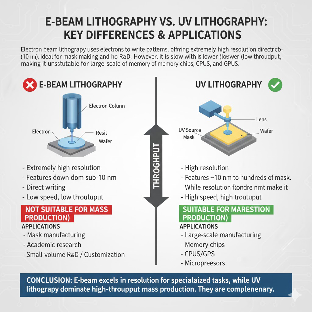
What is the major difference between e-beam lithography and UV lithography?
E-beam lithography directly writes patterns using electrons, achieving extremely high resolution down to sub-10 nm. It is ideal for mask fabrication and R&D, but its low throughput makes it unsuitable for large-scale mass production.
Exposure and Alignment Technology
Resolution and mask durability comparison among exposure modes
Resolution: Vacuum + Hard Contact > Vacuum Contact > Hard Contact > Soft Contact > Proximity
Mask durability: Proximity > Soft Contact > Hard Contact > Vacuum Contact > Vacuum + Hard Contact
How many exposure modes are there?
Exposure modes include soft contact, hard contact, proximity, and vacuum contact.
- Soft Contact: Chuck rises to leveling height; wafer contacts mask
- Hard Contact: Wafer contacts mask; wafer vacuum is released and positive nitrogen pressure is applied
- Vacuum Contact: Vacuum ring creates a vacuum environment between wafer and mask
- Proximity: Wafer and mask maintain a fixed gap
What do the pre-exposure contact modes mean?
What is the basic principle of wafer and mask leveling?
The wafer rests on a three-point overpressure leveling mechanism. Upon contact with the mask, the mechanism acts like a spring to achieve planarity, then locks to maintain stable alignment.
How is alignment and exposure gap control achieved?
The leveling mechanism is mounted on a Z-axis drive system, allowing controlled vertical movement to set the wafer–mask gap after leveling and locking.
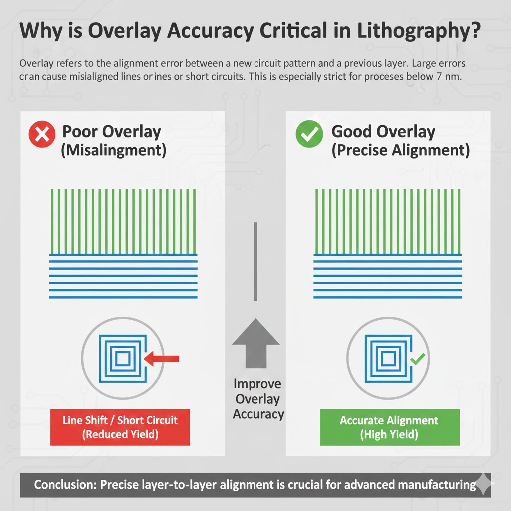
What does overlay accuracy mean in exposure tools?
Overlay refers to the alignment error between a new circuit layer and the previous layer. Excessive error can cause misalignment or short circuits, especially critical below 7 nm nodes.
What is automatic alignment in contact exposure tools?
Automatic alignment uses optical systems and image recognition to align mask patterns with existing wafer patterns, greatly improving accuracy and efficiency.
Why is automatic alignment important?
Multi-layer processes require precise alignment. Automatic alignment ensures accurate pattern stacking, improves yield, and reduces manual adjustment time.
What is the typical accuracy of automatic alignment?
Front-side alignment accuracy: within ±0.5 µm
Back-side alignment accuracy: within ±1 µm
Sufficient for MEMS, optoelectronics, PCB, and selected semiconductor applications.
How does automatic alignment work?
The system captures wafer alignment keys, compares them with mask alignment marks, calculates the optimal position, and performs fine stage adjustments to achieve precise overlay.
- Faster processing
- Higher accuracy
- Better stability
- Suitable for mass production
What are the advantages of automatic alignment over manual alignment?
Is automatic alignment suitable for all processes?
It is essential for multilayer products such as MEMS, biomedical chips, LEDs, and optoelectronic devices. For single-layer or low-precision applications, manual alignment may reduce costs.
- Sub-micron alignment accuracy with high-resolution imaging
- Multiple alignment algorithms
- User-friendly interface with automatic and semi-automatic modes
- High stability for long-term mass production
What are the features of our automatic alignment system?
Photoresist, Coating, Development, and Cleaning
What factors affect film thickness in spin coating?
Spin speed (rpm), solution viscosity, coating time, ambient temperature, and humidity.
What are the types and functions of baking?
1. Soft bake: Removes solvents and improves adhesion
2. Post-exposure bake (PEB): Promotes acid diffusion and improves resolution
3. Hard bake: Enhances etch resistance and film strength
What are the pros and cons of different development methods?
1. Immersion: High uniformity, high chemical usage, suitable for large panels
2. Dipping: Full coverage, chemical waste, batch production
3. Spin-Puddle: Low chemical usage, requires precise timing and speed control
4. Spin-Spray: Fast processing, complex equipment, precise nozzle and speed control
What parameters should be considered for spin coaters?
Film thickness uniformity and spin speed control accuracy.
What parameters should be considered for developers?
Uniform chemical distribution, development time, and drying temperature control accuracy.
What parameters should be considered for rinsing equipment?
Cleaning methods (wet, dry, ultrasonic, or spin cleaning) and particle removal efficiency.