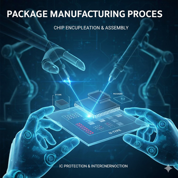
Packaging processes
Semiconductor packaging processes serve as the critical bridge between wafer manufacturing and system-level applications, covering chip dicing, bonding, interconnection, encapsulation, redistribution layers (RDL), and testing. The core objective is to ensure reliable electrical connections, mechanical integrity, and thermal performance under high-precision and high-reliability requirements.
M&R Technology focuses on photolithography-related equipment for semiconductor manufacturing, supporting packaging process engineers during R&D validation and mass production by maintaining pattern accuracy, alignment stability, and overall process consistency to ensure packaging quality and yield performance.
The role of packaging processes is to connect semiconductor chips to external circuits while ensuring signal integrity and effective thermal dissipation. Traditional packaging methods are primarily based on wire bonding and flip-chip technologies. However, as chip designs become increasingly complex, advanced packaging technologies have gradually become mainstream, including 2.5D and 3D packaging, CoWoS, Foveros, and fan-out solutions. These processes not only involve dicing, die attachment, and metal interconnections, but also encompass thermal structure design and the selection of packaging materials. Applications span high-performance computing, AI chips, 5G communications, and automotive electronics. Because advanced packaging enables the integration of more functions within limited space while improving signal speed, it is regarded as a key approach to overcoming the limitations of Moore’s Law. Current packaging process development focuses on enhancing thermal efficiency, reducing interconnect latency, and improving overall system reliability.
Key Challenges in Semiconductor Packaging
As packaging technologies evolve toward higher density, greater integration, and miniaturization, packaging processes face increasingly stringent challenges, including fine-line RDL, micro-pitch interconnects, warpage control, and multi-die integration.
Even minor process deviations can lead to electrical failures, reduced structural reliability, or yield fluctuations, making process stability and equipment repeatability critical success factors in semiconductor packaging.
The Role of Photolithography Equipment in Semiconductor Packaging
Photolithography equipment plays a key role in semiconductor packaging by defining and aligning redistribution layers (RDL), bump openings, and packaging structure patterns.
Stable exposure energy, highly uniform coating and development performance, and precise alignment accuracy are essential for linewidth control, interlayer registration, and the reliability of subsequent metallization processes.
Process Requirement Differences Among Packaging Technologies
Different packaging technologies impose distinct requirements on photolithography and related process equipment.
Conventional packaging emphasizes process stability and cost efficiency, while advanced packaging technologies such as Fan-Out, 2.5D/3D IC, and wafer-level packaging require high-resolution patterning, precise alignment, and robust multilayer process control.
In advanced packaging applications, equipment precision, stability, and repeatability are key enablers for successful process development and high-volume manufacturing.
M&R Technology’s Equipment Support for Semiconductor Packaging
To address the requirements of semiconductor packaging, M&R Technology provides comprehensive photolithography process equipment solutions, including exposure, coating, developing, cleaning, surface treatment, and metrology systems.
These solutions help packaging engineers maintain stable pattern transfer quality and alignment accuracy across different packaging architectures. Through flexible equipment configurations and professional process support, M&R Technology enables R&D development, process validation, production line deployment, and mass production applications.
Application Industries
Semiconductor packaging processes are widely applied across consumer electronics, automotive electronics, artificial intelligence, high-performance computing, communications, and advanced system integration industries, all of which demand high levels of reliability, packaging density, and manufacturing stability.