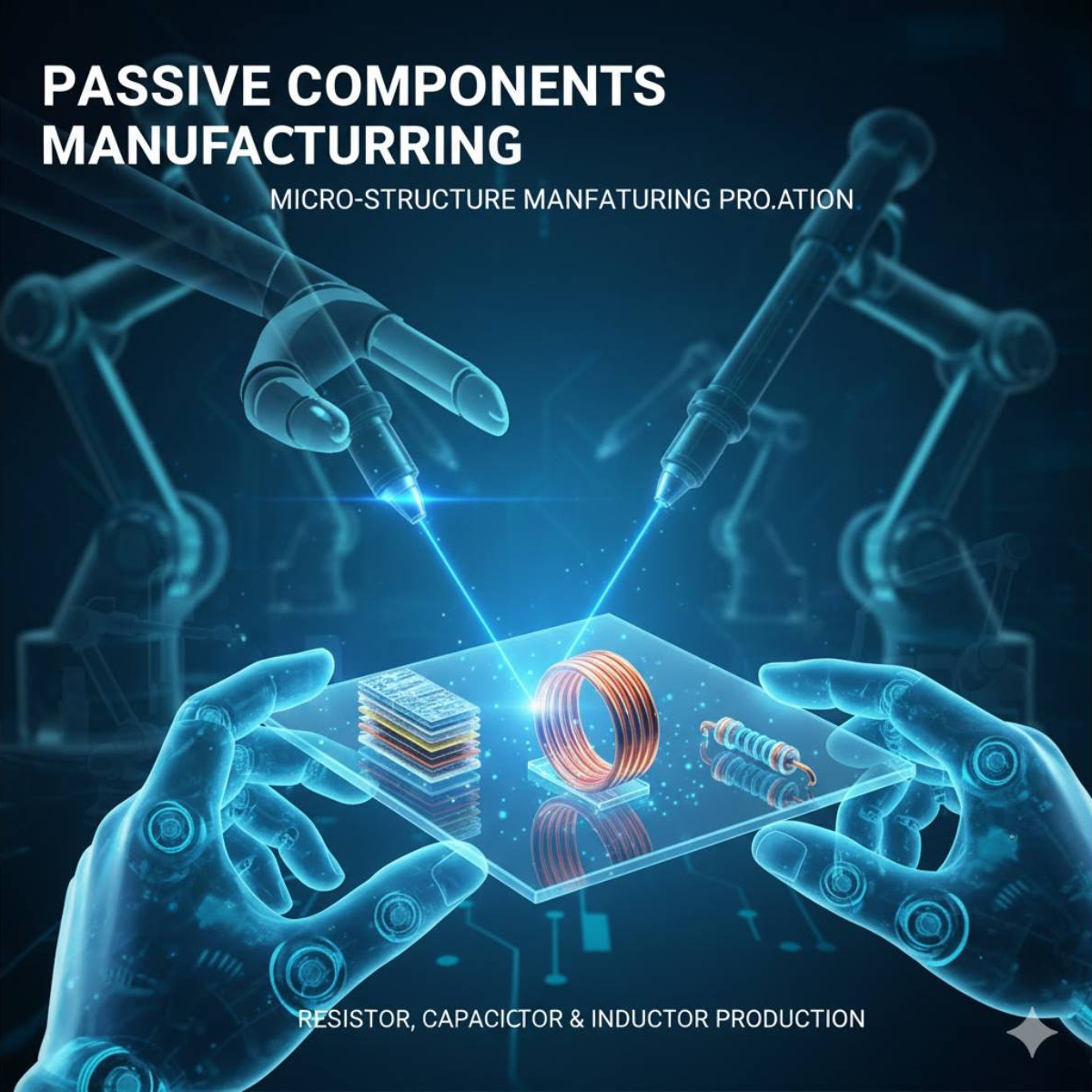
Passive component manufacturing processes
Passive components manufacturing processes cover key electronic components such as resistors, capacitors, inductors, and multilayer ceramic components. The core objective is to achieve material formation, thin-film deposition, pattern definition, and multilayer structure integration under high-precision and high-stability conditions to ensure consistent electrical performance and reliability.
M&R Technology focuses on photolithography-related equipment, supporting passive component process engineers during both R&D introduction and mass production by maintaining pattern accuracy, process stability, and repeatability to ensure component performance meets system-level requirements.
Passive component manufacturing primarily covers the production of resistors, capacitors, and inductors. Although these components are relatively simple in size, they play a critical role in the stability of electronic systems. Common processes include ceramic powder forming and sintering, thin-film deposition, electrode printing, and surface treatment. As products continue to move toward higher frequencies and miniaturization, passive components must maintain precise electrical characteristics—such as low equivalent series resistance (ESR) or high Q factor—within increasingly smaller form factors. Passive components are widely used in smartphones, networking and communication equipment, servers, and automotive electronics. Due to their broad application range and steady demand, control over material purity, structural consistency, and long-term reliability has become a key factor in enhancing product competitiveness.
Key Challenges in Passive Components Manufacturing
As electronic products continue to evolve toward higher density, miniaturization, and high-frequency operation, passive components manufacturing faces increasingly stringent challenges, including fine electrode structures, material consistency, multilayer stacking control, and yield management.
Even minor process deviations can result in electrical parameter drift, reduced reliability, or yield fluctuations, making process stability and equipment consistency critical success factors for high-volume manufacturing.
The Role of Photolithography Equipment in Passive Components Manufacturing
Photolithography equipment plays a critical role in passive components manufacturing by defining electrode structures, circuit patterns, and functional layers with precise alignment control.
Stable exposure energy, highly uniform coating and development performance, and accurate alignment capability are essential to ensuring electrode dimension control, multilayer registration, and consistent electrical characteristics.
Process Requirement Differences Among Passive Components
Different types of passive components impose distinct requirements on photolithography and related process equipment.
Resistors emphasize linewidth control and resistance stability; capacitors require precise dielectric thickness control and electrode alignment accuracy; inductors demand robust circuit structures and high process repeatability.
As a result, equipment stability and repeatability are key enablers for successful process development and mass production of passive components.
M&R Technology’s Equipment Support for Passive Components Manufacturing
To address the requirements of passive components manufacturing, M&R Technology provides comprehensive photolithography process equipment solutions, including exposure, coating, developing, cleaning, surface treatment, and metrology systems.
These solutions help process engineers maintain stable pattern transfer quality and robust process control across different component structures and material conditions. Through flexible equipment configurations and professional process support, M&R Technology supports R&D development, process validation, production line deployment, and mass production applications.
Application Industries
Passive components manufacturing processes are widely applied across consumer electronics, automotive electronics, communications equipment, industrial electronics, artificial intelligence, and high-performance computing industries, all of which demand high levels of reliability, electrical stability, and manufacturing consistency.