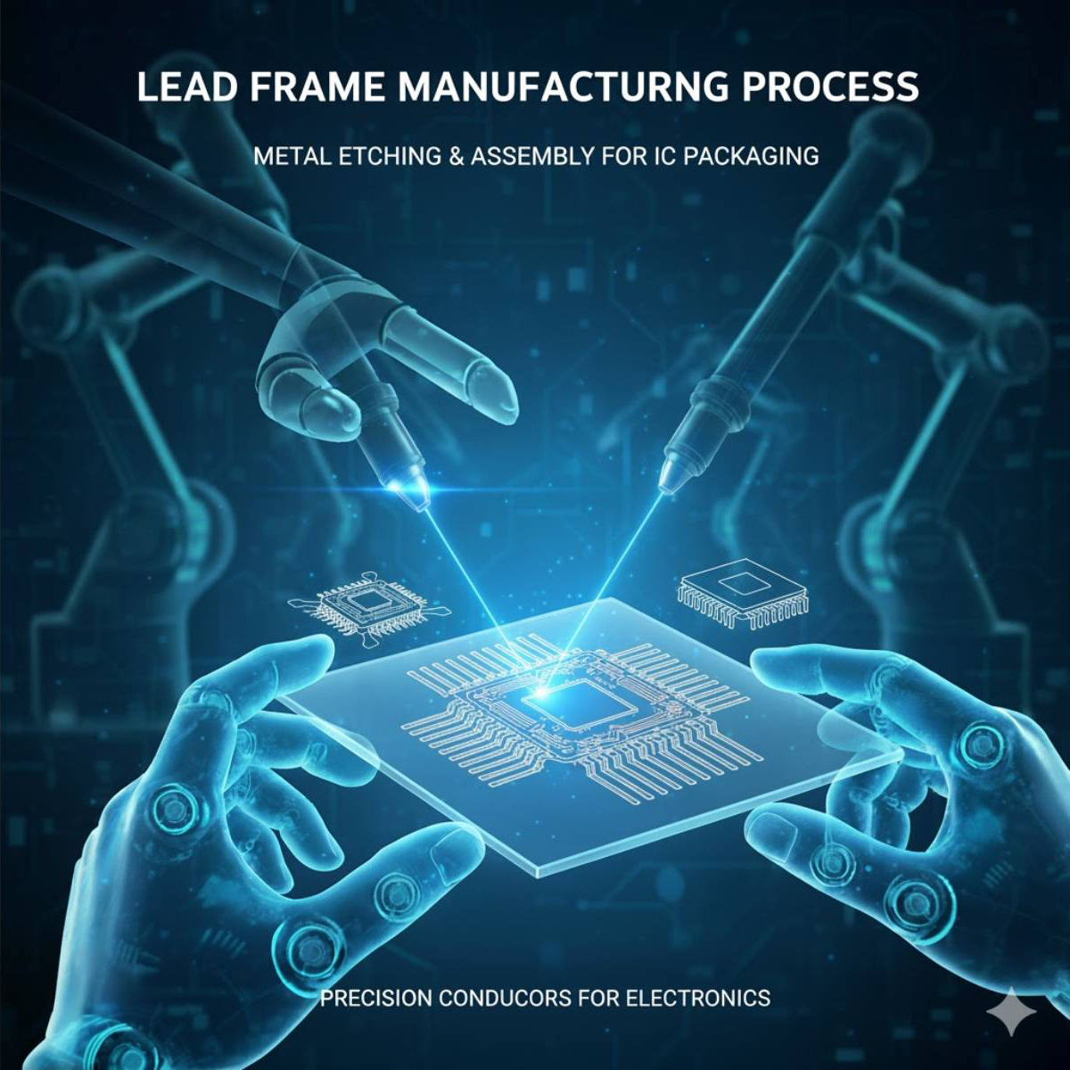
Lead frame manufacturing process
Leadframe manufacturing is a critical foundational process in semiconductor packaging, primarily applied to IC leadframes. The core objective is to achieve precise and consistent metal patterning, etching, stamping, and surface treatment under high-precision conditions to ensure reliable electrical conductivity, mechanical support, and thermal performance.
M&R Technology focuses on photolithography-related equipment, supporting leadframe process engineers during both R&D introduction and mass production by maintaining pattern accuracy, linewidth control, and overall process stability to ensure leadframe quality and packaging yield.
Lead frame manufacturing primarily includes metal stamping, chemical etching, electroplating, and forming processes. Its function is to support semiconductor chips and provide electrical conduction paths, making it an indispensable foundation in traditional semiconductor packaging. As chip designs continue to move toward miniaturization and higher performance, lead frames are required to offer fine pitch, high precision, and effective thermal dissipation. Today, lead frames are widely used in consumer electronics, automotive electronics, power management, and power semiconductor applications. Although lead frames play a largely hidden role within packaging structures, they have a significant impact on overall electrical performance and reliability. As market demand increasingly emphasizes both high reliability and cost efficiency, lead frame manufacturing processes continue to evolve toward multilayer structures and the use of high-conductivity materials.
Key Challenges in Leadframe Manufacturing
As semiconductor packaging continues to evolve toward higher density, miniaturization, and higher power handling, leadframe manufacturing faces increasingly stringent challenges, including fine-line structures, metal thickness control, warpage management, and surface quality consistency.
Even minor process deviations can result in abnormal electrical resistance, reduced packaging reliability, or yield fluctuations, making equipment stability and process repeatability critical success factors.
The Role of Photolithography Equipment in Leadframe Manufacturing
Photolithography equipment plays a key role in leadframe manufacturing by defining metal patterns, forming etch masks, and controlling precise alignment.
Stable exposure energy, uniform coating and development performance, and high-precision alignment accuracy are essential to ensuring metal linewidth control, pattern consistency, and successful downstream etching processes.
Process Requirement Differences Among Leadframe Technologies
Different leadframe structures and applications impose distinct requirements on process control and equipment capabilities.
Conventional leadframes emphasize high throughput and cost efficiency, while high-power and automotive leadframes require robust processing of thick copper materials, precise linewidth control, and high surface reliability.
In advanced packaging and high-reliability applications, equipment stability, precision, and repeatability are key enablers for successful process development and mass production.
M&R Technology’s Equipment Support for Leadframe Manufacturing
To meet the requirements of leadframe manufacturing, M&R Technology provides comprehensive photolithography process equipment solutions, including exposure, coating, developing, cleaning, surface treatment, and metrology systems.
These solutions help engineers maintain stable pattern transfer quality and robust process control across different material and structural conditions. Through flexible equipment configurations and professional process support, M&R Technology supports R&D development, process validation, production line deployment, and mass production applications.
Application Industries
Leadframe manufacturing processes are widely applied across consumer electronics, automotive electronics, power semiconductors, industrial control, and communication equipment industries, all of which demand high levels of electrical reliability, structural strength, and manufacturing stability.