Equipment Integration Service Case
Comprehensive Photolithography Lab Integration for a Stable, High-Performance Semiconductor Process Environment
This case highlights M&R Technology’s equipment integration service designed for semiconductor wafer manufacturing, with a particular focus on photolithography process laboratories. Leveraging more than 20 years of technical expertise and hands-on experience, M&R provides comprehensive planning and implementation services to help customers build high-performance, stable, and future-expandable process environments that support both current R&D needs and long-term development goals.
Background and Requirement Definition
As semiconductor manufacturing continues to advance, photolithography laboratories play a critical role in product development and process optimization. When establishing or upgrading such facilities, customers must balance equipment completeness, process flow efficiency, and future scalability.
Without an integrated planning approach, laboratories may suffer from inefficient equipment utilization, poor workflow design, or increased costs for future modifications. As a result, the customer required a holistic integration solution covering both equipment and infrastructure.
Engineering Constraints and Integration Challenges
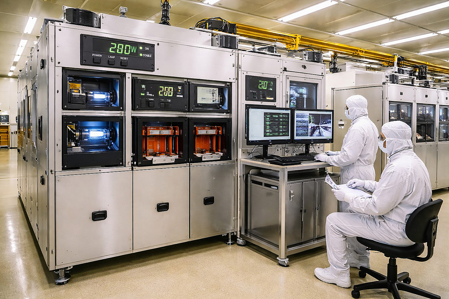
Integrating a photolithography laboratory involves multiple critical process tools, as well as careful consideration of space utilization, process flow, operator efficiency, and facility system compatibility.
Under limited space conditions, ensuring smooth transitions between pre-processing, photolithography, and post-inspection stages presents a major challenge. At the same time, the overall design must retain flexibility for future process upgrades and equipment expansion.
Integration Strategy and Technical Implementation
At the early stage of the project, M&R Technology worked closely with the customer to understand specific product development and process optimization requirements, forming the basis for a comprehensive laboratory layout plan.
The integration solution covered the entire process flow, from pre-processing and photolithography to post-process inspection, ensuring seamless connectivity between each stage. Key equipment included optical microscopes, coaters, exposure systems, developers, plasma cleaning tools, hot plates, vacuum ovens, and other essential photolithography tools. Functional zones were defined according to process steps to improve operational accuracy and efficiency.
In addition, the service scope included cleanroom construction and facility system configuration (water, electricity, and gas), creating an optimal environment for stable process operation.
Implementation Results and Practical Benefits
Through systematic integration planning, the overall laboratory setup timeline was significantly shortened. Equipment installation and qualification were completed smoothly, effectively reducing downtime risks associated with improper configuration.
Process stability and equipment utilization efficiency were improved, allowing the laboratory to quickly transition into R&D and process verification activities.
Engineering Value and Customer Benefits
This equipment integration service enabled the customer to establish a standardized and well-structured photolithography laboratory, improving process stability and yield while preserving flexibility for future expansion.
By providing a single-point integration solution, M&R Technology helped reduce project risk and management complexity, clearly demonstrating its engineering value in semiconductor photolithography process integration.
Engineering Conclusion
Through deep process knowledge and strong system integration capabilities, M&R Technology successfully delivered a comprehensive photolithography laboratory integration project. The resulting environment offers high efficiency, reliability, and scalability, positioning the customer for sustained success in semiconductor process development.