
Wafer cleaning machine | M&R NANO TECHNOLOGY Semiconductor & Optoelectronic Process Equipment
The wafer cleaning machine is suitable for 4-inch to 12-inch wafers and other square or fragmented adsorption stages. It uses cleaning fluid and is equipped with a solvent container with controllable liquid level and a solvent replacement drawer. M&R's wafer cleaning machine features a built-in vacuum generator and automatic drainage device. It uses a two-fluid nozzle to enhance the cleaning effect and offers a pure nitrogen cleaning and drying process. The programmable controller can be equipped with a Chinese/English display board. Non-standard work trays are available upon request, providing various cleaning application modes.
Wafer cleaning machines offer high efficiency and stability in contamination control, making them an indispensable key piece of equipment for any organization seeking to improve process quality, yield, and stability. Choose M&R NANO TECHNOLOGY for high-quality semiconductor & optoelectronic process equipment and reliable customized manufacturing.
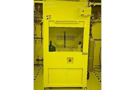
Wafer cleaning machine
The wafer cleaning machine is suitable for 4-inch to 12-inch wafers and other square or fragmented adsorption stages. It uses cleaning fluid and is equipped with a solvent container with controllable liquid level and a solvent replacement drawer. M&R's wafer cleaning machine features a built-in vacuum generator and automatic drainage device. It uses a two-fluid nozzle to enhance the cleaning effect and offers a pure nitrogen cleaning and drying process. The programmable controller can be equipped with a Chinese/English display board. Non-standard work trays are available upon request, providing various cleaning application modes.
Wafer cleaning machines offer high efficiency and stability in contamination control, making them an indispensable key piece of equipment for any organization seeking to improve process quality, yield, and stability.
Equipment Features
Wafer cleaning machines play a crucial role in maintaining surface cleanliness in semiconductor and micro/nano processes and are indispensable equipment for ensuring stable quality in photolithography, thin film deposition, etching, and packaging. Its main feature is the effective removal of particles, metal ions, organic matter, and process residues through a multi-stage process involving chemical solutions, ultrasonic cleaning, rotary spraying, and drying. This provides a high-cleanliness wafer surface, ensuring uniformity and reliability in subsequent processes.
- Cleaning Capacity: Used to remove contaminants from the wafer surface at various processing stages, ensuring process cleanliness and yield.
- Automation Level: From fully automatic, semi-automatic to manual, customizable to meet specific needs.
- Drying Technology: Compatible with other rotary dryer systems and controls.
- Anti-static Function: Includes material selection, anti-static features, and monitoring.
- Waste Discharge Function: May be equipped with a high-efficiency chemical recovery system, enabling partial recovery and reuse of chemicals to reduce chemical usage costs and waste volume.
Specifications
- 4-12 inch fully automatic cleaning machine
- 4-12 inch semi-automatic cleaning machine
- 4-12 inch manual cleaning machine
Configuration
- High-pressure pure water cleaning (two-fluid process)
- Nitrogen purification
- Drying
Options
- FFU (Fan Filter Unit).
- FFU air filter differential pressure monitoring.
- Static eliminator.
- Static electricity detection and monitoring.
- Ultrasonic oscillator and communication.
- Non-standard workpiece trays available upon request.
Applications
- Pre-lithography Cleaning: Removes particles, metal ions, and organic contaminants from the wafer surface, ensuring uniform photoresist coating and improving exposure quality.
- Post-lithography Cleaning (Developing/Etching Residue): Removes residual photoresist debris after development and etching byproducts, ensuring accurate linewidth and process stability.
- Pre- and Post-Thin Film Deposition Cleaning: Applied before and after PVD, CVD, and ALD processes to remove surface contaminants and improve film adhesion and consistency.
- Intermediate Cleaning in Wafer Fabrication: Cleans after each critical step to prevent contamination buildup and quality degradation.
- MEMS Process and Micro/Nano Structure Cleaning: Removes residues or drying marks from microstructures, maintaining the functionality of micro-devices.
- Optoelectronic Components and Sensor Manufacturing: Removes process residues, improving optical transparency and electrical stability.
 Download
 Hot Products
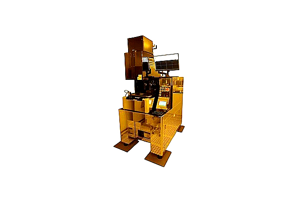


Wafer cleaning machine Professional Custom Semiconductor & Optoelectronic Process Equipment
M&R NANO TECHNOLOGY provides high-quality Wafer cleaning machine and semiconductor & optoelectronic process equipment designed for advanced semiconductor, optoelectronic, and testing applications. Our product line includes detailed Mask Aligners, Spin Coaters, and Developers manufactured in our Taoyuan, Taiwan facility with strong automation capabilities.
We focus on delivering stable quality and precise customization through our in-house R&D and miniaturization technology. This ensures that every system meets strict process requirements while maintaining practical durability, low cost, and high efficiency for end-users.
For global buyers, M&R NANO TECHNOLOGY offers dependable manufacturing support that simplifies the sourcing process. We provide responsive communication, efficient automation integration, and consistent after-sales maintenance to help customers successfully bring their semiconductor & optoelectronic process equipment into production.