Photomask | M&R NANO TECHNOLOGY Semiconductor & Optoelectronic Process Equipment
M&R provides high-resolution, low-defect photomask manufacturing services to support MEMS, optoelectronics, sensors, and semiconductor lithography processes. By using high-flatness substrates and high-quality chromium (Cr) films, M&R ensures precise pattern transfer during exposure, helping customers improve lithography success rates and shorten R&D and pilot production cycles. Whether for process development, prototyping, or small-volume production, M&R delivers stable and reliable photomask support.
In terms of materials and fabrication quality, M&R offers customized photomask solutions based on customer layout and process requirements. High-flatness quartz or glass substrates are combined with optically stable chromium or specialized optical materials to support pattern transfer from micron-scale to nanometer-scale features. In addition, M&R provides comprehensive pre- and post-processing services, including layout inspection, data conversion, dimensional verification, and defect inspection, allowing customers to focus on process development and production ramp-up with confidence. Fast turnaround time and consistent quality have made M&R a long-term photomask partner for both academic institutes and industrial customers. Choose M&R NANO TECHNOLOGY for high-quality semiconductor & optoelectronic process equipment and reliable customized manufacturing.
Photomask
M&R provides high-resolution, low-defect photomask manufacturing services to support MEMS, optoelectronics, sensors, and semiconductor lithography processes. By using high-flatness substrates and high-quality chromium (Cr) films, M&R ensures precise pattern transfer during exposure, helping customers improve lithography success rates and shorten R&D and pilot production cycles. Whether for process development, prototyping, or small-volume production, M&R delivers stable and reliable photomask support.
In terms of materials and fabrication quality, M&R offers customized photomask solutions based on customer layout and process requirements. High-flatness quartz or glass substrates are combined with optically stable chromium or specialized optical materials to support pattern transfer from micron-scale to nanometer-scale features. In addition, M&R provides comprehensive pre- and post-processing services, including layout inspection, data conversion, dimensional verification, and defect inspection, allowing customers to focus on process development and production ramp-up with confidence. Fast turnaround time and consistent quality have made M&R a long-term photomask partner for both academic institutes and industrial customers.
M&R Photomask Capabilities and Service Advantages
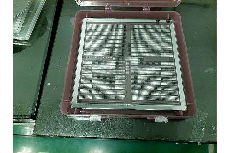
M&R offers photomask fabrication and complete technical support services, including both main masks for original pattern generation and reproduce masks for duplication purposes. Photomask sizes cover common industry standards, typically ranging from 4 inches to 9 inches, with support for extra-large masks up to 24 inches upon request. A wide selection of substrate materials is available, including soda-lime glass, quartz, fused quartz, as well as specialty options such as Mylar film and emulsion masks, to meet diverse process requirements.
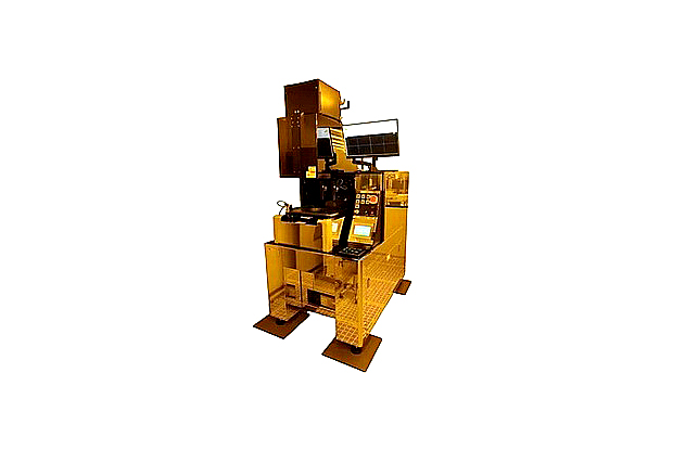
Photomask fabrication follows a rigorous six-step workflow, from CAD design and CAM data conversion to fabrication, cleaning, inspection, and final shipment, ensuring consistent quality and process reliability. In addition, leveraging over 25 years of experience in photolithography processes, M&R also provides advanced mask replacement solutions for contact lithography systems. Through optimized mechanical design, vacuum chuck platforms, and precision alignment modules such as three-point leveling pins, M&R enables fast and accurate mask positioning. This solution is compatible with semi-automatic exposure systems for 2-inch to 12-inch wafers, further improving alignment stability and operational efficiency.
Hot Products

Photomask Professional Custom Semiconductor & Optoelectronic Process Equipment
M&R NANO TECHNOLOGY provides high-quality Photomask and semiconductor & optoelectronic process equipment designed for advanced semiconductor, optoelectronic, and testing applications. Our product line includes detailed Mask Aligners, Spin Coaters, and Developers manufactured in our Taoyuan, Taiwan facility with strong automation capabilities.
We focus on delivering stable quality and precise customization through our in-house R&D and miniaturization technology. This ensures that every system meets strict process requirements while maintaining practical durability, low cost, and high efficiency for end-users.
For global buyers, M&R NANO TECHNOLOGY offers dependable manufacturing support that simplifies the sourcing process. We provide responsive communication, efficient automation integration, and consistent after-sales maintenance to help customers successfully bring their semiconductor & optoelectronic process equipment into production.