
Laser Direct Imaging (LDI) System | M&R NANO TECHNOLOGY Semiconductor & Optoelectronic Process Equipment
Laser Direct Imaging (LDI) is a technology that uses laser light to directly draw patterns on photoresist, eliminating the need for traditional photomask fabrication. It is widely used in PCB manufacturing, semiconductor lithography, and thin-film devices, offering advantages such as high precision, flexibility, speed, and suitability for small-batch production.
Laser Direct Imaging (LDI) systems convert digital design data directly into exposure patterns using high-precision laser sources, optical scanning systems, and precision motion platforms, eliminating the need for traditional photomasks. This maskless approach simplifies process flow, shortens design change and production preparation cycles, and reduces costs and risks associated with mask fabrication and handling. With exposure resolution reaching micron and sub-micron levels, LDI systems meet the requirements of high-density PCB manufacturing, semiconductor lithography, thin-film devices, and MEMS applications. LDI platforms support a wide range of substrate materials and sizes and incorporate automatic focus control and multi-point alignment to maintain stable exposure performance across varying surface profiles and thicknesses. By combining high resolution, process flexibility, and rapid design iteration capability, LDI has become an effective exposure solution for R&D, rapid prototyping, and small-to-medium batch production environments that demand precision, efficiency, and adaptability. Choose M&R NANO TECHNOLOGY for high-quality semiconductor & optoelectronic process equipment and reliable customized manufacturing.
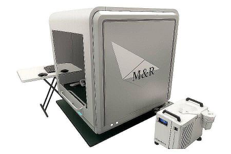
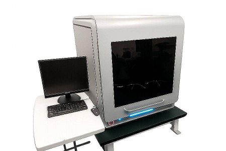
Laser Direct Imaging (LDI) System
Laser Direct Imaging (LDI) is a technology that uses laser light to directly draw patterns on photoresist, eliminating the need for traditional photomask fabrication. It is widely used in PCB manufacturing, semiconductor lithography, and thin-film devices, offering advantages such as high precision, flexibility, speed, and suitability for small-batch production.
Laser Direct Imaging (LDI) systems convert digital design data directly into exposure patterns using high-precision laser sources, optical scanning systems, and precision motion platforms, eliminating the need for traditional photomasks. This maskless approach simplifies process flow, shortens design change and production preparation cycles, and reduces costs and risks associated with mask fabrication and handling. With exposure resolution reaching micron and sub-micron levels, LDI systems meet the requirements of high-density PCB manufacturing, semiconductor lithography, thin-film devices, and MEMS applications. LDI platforms support a wide range of substrate materials and sizes and incorporate automatic focus control and multi-point alignment to maintain stable exposure performance across varying surface profiles and thicknesses. By combining high resolution, process flexibility, and rapid design iteration capability, LDI has become an effective exposure solution for R&D, rapid prototyping, and small-to-medium batch production environments that demand precision, efficiency, and adaptability.
Advantages of M&R's LDI Exposure Machine
M&R's desktop LDI exposure system is a compact laser direct-write system (SCLDI) developed specifically for experimental research, rapid prototyping, and small-batch production. Its core function is to directly draw the desired circuit patterns onto a photoresist-coated substrate using a high-precision laser beam, replacing traditional photomask exposure. This effectively reduces photomask manufacturing costs and time, and offers advantages such as high precision, flexibility, and speed; design modifications only require changes to the drawing file.
- Core Performance and Specifications: This desktop LDI system provides excellent lithography capabilities, suitable for 2- to 6-inch wafers (including prismatic wafers) with substrate thicknesses ranging from 0.3 to 6 mm.
- Resolution and Accuracy: The system boasts extremely high resolution; at 20X objectives, the minimum linewidth (CD) can reach ≥0.8µm, and the CD uniformity (CDU) is better than ≤ ±0.15µm. The highest stitching accuracy can be controlled to ≤0.2µm, and the data resolution is ≥20 nm.
- Alignment capability: The system supports multi-layer pattern alignment, achieving an overlay accuracy of ≤ ±0.5µm with a 20X objective.
- Writing efficiency: Although designed for R&D, it still possesses a certain level of efficiency; for example, with a 4X objective, the writing efficiency can reach 240 mm²/min (based on a 6-inch wafer).
- Technical architecture and modules: This LDI system employs an integrated design to ensure exposure stability and accuracy.
- Light source and optics: The standard configuration is a 10 W@405nm laser light source, with a 2W@375nm option available upon request. The system features fully automatic switching between 4X, 10X, and 20X objectives.
- High-precision motion platform: Utilizing a high-precision marble base (flatness requirement ≥3µm) and a closed-loop direct-drive linear platform (accuracy 20 nm) as the core motion base. Autofocus and Stability: Equipped with Real-time Autofocus (AF) achieving an accuracy of 800 nm at 20X zoom. The system also features multiple vibration isolation protections, periodic automatic calibration, and water-cooled environmental control, along with simultaneous temperature and humidity monitoring to ensure process stability.
- Operation and Software: Manual loading is employed; recommended for use in a Class 1000 cleanroom. The control software is self-developed and supports multiple data formats including Gerber274, GDS, and DXF.
M&R's SCLDI system offers extremely high precision and design flexibility, effectively addressing issues such as high mask costs, slow process changeovers, and insufficient pattern accuracy. It is an ideal choice for teams and research and development environments seeking flexibility, efficiency, and high lithography quality, enabling rapid prototyping and multi-layer exposure alignment.
Specifications
- Substrate Type: Wafer
- Substrate Size: 2 - 6 inches, minimum 12mm x 12mm, maximum 150mm x 150mm
- Substrate Thickness: 0.3~6 mm
- Minimum Linewidth (CD): ≥3μm @4X, ≥1.5μm @10X, ≥0.8μm @20X
- CD Uniformity (CDU): ≤±0.3 @4X 3μm, ≤±0.2 @10X 1.5μm, ≤±0.15 @20X 0.8μm
- Splicing: ≤0.2μm
- Alignment Accuracy: 4X ≤±1μm
- Alignment Accuracy: 10X ≤±1μm
- Alignment Accuracy: 20X ≤±0.5μm
- Target Recognition: Circular Pad, Cross Mark, other types available for upgrade
- Alignment Mode: Global or Local
- Writing Efficiency: 4 x 240mm²/min @6inch
- Writing Efficiency: 10 x 60mm²/min @6inch
- Writing Efficiency: 20 x 15mm²/min @6inch
- Objective Lens Switching: Automatic
- Light Source Type: 10W @405 nm, customizable 2W @375nm
- Laser Lifespan: 8000H, 50% degradation defines unusable
- Loading and Unloading: Manual
- AF (Instant Focusing Module) Range: 0~150μm
- Travel: 10mm
- 4X Accuracy: 8000nm
- 10X Accuracy: 1500nm
- 20X Accuracy: 800nm
- Platform - High-Precision Marble Base: Flatness ≥3μm
- Motorized Stage Type: Closed-Loop Direct Drive Linear Platform (Screwless)
- Travel: 200mm
- Accuracy: 20nm (encoder resolution)
- Bidirectional Accuracy: ±300nm
- Rotary stage, automatically adjusted (linear stage)
- Equipment Dimensions: Main unit: 95cm x 85cm x 100cm ±50mm
- Data Formats: Gerber274, ODB++, GDS, DXF
- Overlay (Front-side alignment): ≤±1μm @4X, ≤±1μm @10X, ≤±0.5μm @20X
Configuration
- Laser light source: Provides high-precision laser beam/optical scanning system/motion platform (X, Y axes)
- Photoresist coating and soft-bake device/autofocus system/control system and software
- Protective cover and safety system/positioning and calibration system
Applications
- Printed Circuit Board (PCB) Manufacturing
- Semiconductor Processes
- Display Panels and Thin-Film Components
- Packaging Technology
- Micro-Electro-Mechanical Systems (MEMS)
- Other High-Precision Lithography Needs
 Download
 Hot Products
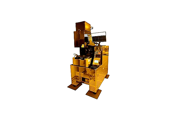


Laser Direct Imaging (LDI) System Professional Custom Semiconductor & Optoelectronic Process Equipment
M&R NANO TECHNOLOGY provides high-quality Laser Direct Imaging (LDI) System and semiconductor & optoelectronic process equipment designed for advanced semiconductor, optoelectronic, and testing applications. Our product line includes detailed Mask Aligners, Spin Coaters, and Developers manufactured in our Taoyuan, Taiwan facility with strong automation capabilities.
We focus on delivering stable quality and precise customization through our in-house R&D and miniaturization technology. This ensures that every system meets strict process requirements while maintaining practical durability, low cost, and high efficiency for end-users.
For global buyers, M&R NANO TECHNOLOGY offers dependable manufacturing support that simplifies the sourcing process. We provide responsive communication, efficient automation integration, and consistent after-sales maintenance to help customers successfully bring their semiconductor & optoelectronic process equipment into production.