Semi-Automatic Developer | M&R NANO TECHNOLOGY Semiconductor & Optoelectronic Process Equipment
The Semi-Automatic developer plays a crucial role in photolithography processes to ensure image quality, making them particularly suitable for research institutions, small-scale production lines, and new product development teams. Their greatest benefit lies in the automated control of developing time, agitation mode, and solution circulation throughout the process, ensuring high consistency in development results and significantly reducing linewidth variations and defects caused by human error. For applications requiring stable reproducibility and precision, they effectively improve yield and shorten process calibration time.
Features include automated fluid flow control, uniform agitation, settable developing parameters, a clean and corrosion-resistant mechanism, and the flexibility of manual film loading and unloading. This allows for both stability and rapid switching between different photoresist and process conditions, making them ideal for highly variable R&D work. Reasons for choosing semi-automatic developing machines typically include: improved developing uniformity, reduced human error, prevention of over- or under-development, shorter experimental cycles, and enhanced process traceability. Compared to manual development, it significantly improves consistency; compared to fully automatic systems, it offers better cost-effectiveness and operational freedom. Typical applications include MEMS fabrication, optoelectronic component manufacturing, sensor development, photoresist material research, and semiconductor-related teaching. Choose M&R NANO TECHNOLOGY for high-quality semiconductor & optoelectronic process equipment and reliable customized manufacturing.
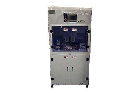
Semi-Automatic Developer
The Semi-Automatic developer plays a crucial role in photolithography processes to ensure image quality, making them particularly suitable for research institutions, small-scale production lines, and new product development teams. Their greatest benefit lies in the automated control of developing time, agitation mode, and solution circulation throughout the process, ensuring high consistency in development results and significantly reducing linewidth variations and defects caused by human error. For applications requiring stable reproducibility and precision, they effectively improve yield and shorten process calibration time.
Features include automated fluid flow control, uniform agitation, settable developing parameters, a clean and corrosion-resistant mechanism, and the flexibility of manual film loading and unloading. This allows for both stability and rapid switching between different photoresist and process conditions, making them ideal for highly variable R&D work. Reasons for choosing semi-automatic developing machines typically include: improved developing uniformity, reduced human error, prevention of over- or under-development, shorter experimental cycles, and enhanced process traceability. Compared to manual development, it significantly improves consistency; compared to fully automatic systems, it offers better cost-effectiveness and operational freedom. Typical applications include MEMS fabrication, optoelectronic component manufacturing, sensor development, photoresist material research, and semiconductor-related teaching.
Advantages of M&R's Semi-Automatic Developer
M&R's semi-automatic developer features an AC servo motor and high-precision speed control, combined with an automatic feeding and nozzle system. It can perform photoresist development, cleaning, and nitrogen drying, and manages multiple recipes via a PLC and touch panel, ensuring stability and repeatability.
M&R's semi-automatic developer combines automation and user-friendly design, featuring a SEMI communication architecture, real-time monitoring system, and safety protection mechanisms, balancing flexibility and stability in operation. Its motor-driven tray system provides high-precision rotation and low flatness error, and combined with the automatic feeding and spraying module, it effectively improves process consistency. Compared to fully automatic systems, semi-automatic models reduce costs while maintaining high efficiency and reliability, making them suitable as a balanced solution between mass production and R&D.
M&R's semi-automatic developer automatically controls development time, liquid flow rate, and agitation method to ensure each wafer receives the same processing conditions, avoiding over-development, under-development, and linewidth variations caused by manual operation. Automated processes replace manual timing and stirring, effectively reducing operational variability, making process results more predictable, and facilitating the establishment of standardized development processes. Retaining manual film loading and material switching, coupled with programmed development control, allows R&D personnel to quickly adjust conditions while maintaining stable results, achieving an ideal balance between R&D and small-scale production. The clear user interface and simplified processes avoid prolonged manual stirring or monitoring, improving work efficiency and safety. It is more cost-effective than fully automated systems, has a corrosion-resistant structure, is easy to maintain, can be used stably for a long time, and has low maintenance costs.
Specifications
- Frame: SUS housing, WPP
- Motor Specification: AC Servo Motor
- Motor Speed: 10-3000 RPM
- Speed Accuracy: Constant speed +/-1%
- Nozzle Mechanism: Automatic feeder and 2-set nozzles for developer, 2-set automatic feeder and 2-set nozzles for DIW & N2
- Applicable Wafer Size: 2”-8”
- Pad Mechanism: Ceramic/acid and alkali resistant, 45-degree bevel to prevent PR penetration
- Pad Flatness: <10um
- Operation Method: Automatic feeding
- Control System: PLC + Touch Panel, 30 configurable recipe modules
- Safety Devices: Pad vacuum leakage protection, vacuum detection, leakage circuit breaker protection
Configuration
- Spindle rotary motor
- Bearing mechanism
- Control system
- Safety devices
- Liquid/pneumatic bearing system
Options
- SEMI Equipment Communication Architecture
- Automatic Pick-and-Place Arm Architecture
- Real-time Monitoring System
Applications
- Suitable for photoresist development processes on 2-inch to 8-inch wafers or substrates
- Semiconductor manufacturing
- Optoelectronic panels
- MEMS and lithography labs
- Especially suitable for small- to medium-scale pilot production and R&D needs
Hot Products

Semi-Automatic Developer Professional Custom Semiconductor & Optoelectronic Process Equipment
M&R NANO TECHNOLOGY provides high-quality Semi-Automatic Developer and semiconductor & optoelectronic process equipment designed for advanced semiconductor, optoelectronic, and testing applications. Our product line includes detailed Mask Aligners, Spin Coaters, and Developers manufactured in our Taoyuan, Taiwan facility with strong automation capabilities.
We focus on delivering stable quality and precise customization through our in-house R&D and miniaturization technology. This ensures that every system meets strict process requirements while maintaining practical durability, low cost, and high efficiency for end-users.
For global buyers, M&R NANO TECHNOLOGY offers dependable manufacturing support that simplifies the sourcing process. We provide responsive communication, efficient automation integration, and consistent after-sales maintenance to help customers successfully bring their semiconductor & optoelectronic process equipment into production.