
Manual Mask Aligner | M&R NANO TECHNOLOGY Semiconductor & Optoelectronic Process Equipment
M&R's manual mask aligners are suitable for 2” to 6” wafers, with an XY travel of up to 200mm. Some models are equipped with electric drives, and the minimum fine-tuning resolution can reach 40 nm. The standard model offers manual 1µm level precision, balancing flexibility and cost-effectiveness. Alignment is achieved through human visual identification, with an alignment accuracy of approximately 1.0~2.0µm, suitable for R&D and experimental applications. Some models offer non-contact exposure, avoiding wafer surface damage and improving sample preservation. The system design is simple, maintenance is easy, and it can be equipped with an IPC control module to provide basic data management and operation interface.
This model is widely used in universities, research institutions, and early-stage process testing in optoelectronics, MEMS, and other fields, helping users to complete the development and verification of exposure processes in the most economical way. Choose M&R NANO TECHNOLOGY for high-quality semiconductor & optoelectronic process equipment and reliable customized manufacturing.
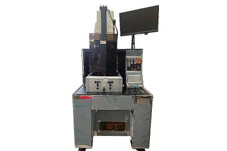


Manual Mask Aligner
M&R's manual mask aligners are suitable for 2” to 6” wafers, with an XY travel of up to 200mm. Some models are equipped with electric drives, and the minimum fine-tuning resolution can reach 40 nm. The standard model offers manual 1µm level precision, balancing flexibility and cost-effectiveness. Alignment is achieved through human visual identification, with an alignment accuracy of approximately 1.0~2.0µm, suitable for R&D and experimental applications. Some models offer non-contact exposure, avoiding wafer surface damage and improving sample preservation. The system design is simple, maintenance is easy, and it can be equipped with an IPC control module to provide basic data management and operation interface.
This model is widely used in universities, research institutions, and early-stage process testing in optoelectronics, MEMS, and other fields, helping users to complete the development and verification of exposure processes in the most economical way.
Advantages of M&R's manual mask aligner
M&R's manual mask aligner is a high-performance exposure device designed for early-stage R&D, laboratory use, and small-scale prototyping. Its biggest feature is its compact, entry-level, desktop design, providing the most flexible and economical lithography solution. The device's small size and ease of installation save experimental space and significantly reduce purchase costs, making it particularly suitable for teams with limited budgets requiring multiple distributed workstations.
Manual operation is a key advantage of this device. The alignment method is intuitive and easy to learn, allowing students, researchers, and engineers to quickly get started and immediately begin process validation. Because there are no complex automated processes, users can freely adjust various parameters, facilitating experimentation, error correction, and process exploration.
For sample protection, some models employ a non-contact design, preventing wafer damage. This is especially beneficial for thin wafers, MEMS structures, or warped wafers, significantly improving experimental success rates and reliability.
It is worth mentioning that M&R's manual mask aligner offers high upgrade flexibility. Users can choose to equip the motorized platform to improve XY axis accuracy to 40 nm, upgrading from manual beginner to advanced verification without replacing the entire system, offering extremely high scalability.
M&R's manual mask aligner provides customers with a flexible and efficient starting point for lithography processes due to its low cost, ease of operation, high stability, and scalability, making it an ideal choice for educational institutions, R&D centers, and startups.
Specifications
- Applicable wafer size: 2”~6”
- XY travel: 200mm
- XY axis accuracy: 40nm motorized / 1µm manual (depending on model)
- Z axis travel: None or simple adjustment mechanism
- Alignment accuracy: 1.0~2.0µm (manual)
- Exposure resolution: 0.8µm~1.0µm
- Alignment method: Human visual identification
- Exposure mode: Non-contact / Contact (depending on model)
- Control system: IPC (some models)
Configuration
- Desktop lightweight design
- Basic exposure control module
- IPC interface (for some models)
Options
- Simple vacuum suction cup photomask mounting
- Customized optical modules
- Basic image-aided alignment system
Applications
- Research institutions and university laboratories
- Initial process development
- Optoelectronics and MEMS R&D
- Small-batch pilot production
 Download
 Hot Products
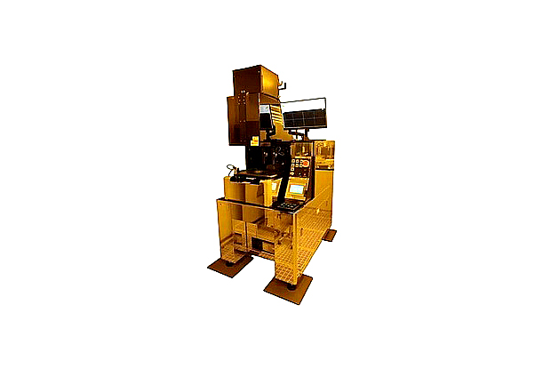

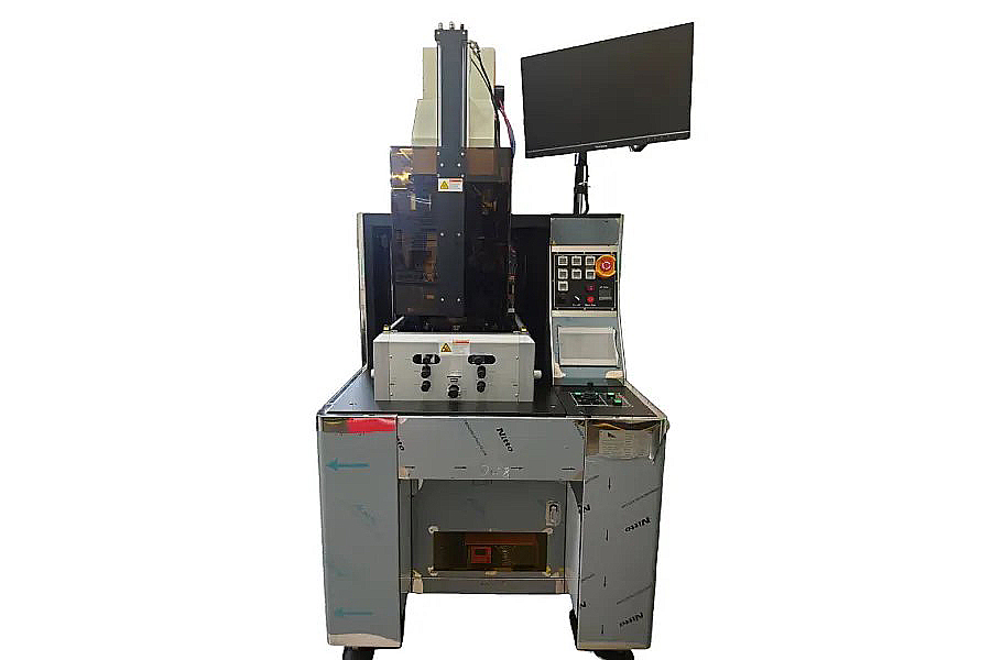
Manual Mask Aligner Professional Custom Semiconductor & Optoelectronic Process Equipment
M&R NANO TECHNOLOGY provides high-quality Manual Mask Aligner and semiconductor & optoelectronic process equipment designed for advanced semiconductor, optoelectronic, and testing applications. Our product line includes detailed Mask Aligners, Spin Coaters, and Developers manufactured in our Taoyuan, Taiwan facility with strong automation capabilities.
We focus on delivering stable quality and precise customization through our in-house R&D and miniaturization technology. This ensures that every system meets strict process requirements while maintaining practical durability, low cost, and high efficiency for end-users.
For global buyers, M&R NANO TECHNOLOGY offers dependable manufacturing support that simplifies the sourcing process. We provide responsive communication, efficient automation integration, and consistent after-sales maintenance to help customers successfully bring their semiconductor & optoelectronic process equipment into production.