Photoresist | M&R NANO TECHNOLOGY Semiconductor & Optoelectronic Process Equipment
M&R provides photoresist solutions covering both thin-film and thick-film lithography applications, supporting a wide range of process requirements including IC manufacturing, advanced packaging, MEMS, and optical components. Through diverse photoresist formulations, these solutions address high-resolution patterning, high aspect ratio structures, metal lift-off processes, and permanent microstructure fabrication, helping customers establish stable and reproducible lithography processes from R&D through volume production. Choose M&R NANO TECHNOLOGY for high-quality semiconductor & optoelectronic process equipment and reliable customized manufacturing.

Photoresist
M&R provides photoresist solutions covering both thin-film and thick-film lithography applications, supporting a wide range of process requirements including IC manufacturing, advanced packaging, MEMS, and optical components. Through diverse photoresist formulations, these solutions address high-resolution patterning, high aspect ratio structures, metal lift-off processes, and permanent microstructure fabrication, helping customers establish stable and reproducible lithography processes from R&D through volume production.
Process & Application Coverage
The KemLab photoresist portfolio spans key lithography applications, ranging from high-resolution thin-film photoresists for IC manufacturing (such as the KL 5300 series), to advanced thick-film photoresists designed for high aspect ratio applications in advanced packaging processes including electroplating, bumping, and TSV (K-PRO™ series). The portfolio also includes materials with excellent chemical and thermal stability for MEMS, microfluidics, and optical component fabrication (SQ and HARE SQ™ series).
In addition, dedicated formulations for metal lift-off processes are available, such as APOL-LO 3200 and KL IR series, enabling stable undercut profiles and reliable metal pattern formation. Overall, these photoresist solutions are widely applied across microelectronics manufacturing, advanced packaging, MEMS, and optical industries, allowing flexible selection according to specific process requirements.
Core Product Categories and Applications
-
Positive Film Photoresists:
- Thin Film Applications: The KL 5300 series is suitable for IC manufacturing, with a film thickness range of 0.2 – 2.0 µm and a resolution up to 0.55 microns. The KL 7000 series is an environmentally friendly positive film photoresist without PFAS.
- Thick Film Applications: The K-PRO™ series (5 – 25+ µm) are advanced thick film positive film photoresists designed for advanced packaging, bumping, TSV, and electroplating, featuring high sensitivity and metal compatibility. The KL 6000 series (2.5 – 12 µm) is also suitable for advanced packaging and can be developed without PEB (Post-Exposure Bake). Negative Photoresists and Special Photoresists:
- Lift-Off: The APOL-LO 3200 series is designed for metal lift-off, creating beveled structures that facilitate metal layer removal. The KL IR series is an image-reversing photoresist, switchable between positive and negative modes for lift-off applications.
- Vertical Structures: The KL NPR series can form vertical sidewall structures with a single-layer thickness of up to 20 µm, exhibiting excellent thermal stability (withstanding 130°C), suitable for TSV, electroplating, and RIE etching.
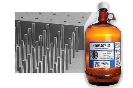
- Permanent Materials: The HARE SQ™ series is an epoxy-based negative photoresist (2–100 µm). Due to its excellent chemical, mechanical, and thermal resistance, it is suitable for fabricating permanent microstructures such as MEMS, microfluidics, waveguides, and pixel walls, and can replace SU-8.
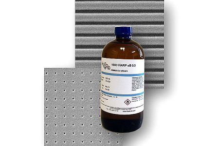
- Electron Beam Resist: HARP™ PMMA Series is designed for high-resolution electron beam direct writing lithography and is suitable for nanoscale patterning.
- Download

Hot Products

Photoresist Professional Custom Semiconductor & Optoelectronic Process Equipment
M&R NANO TECHNOLOGY provides high-quality Photoresist and semiconductor & optoelectronic process equipment designed for advanced semiconductor, optoelectronic, and testing applications. Our product line includes detailed Mask Aligners, Spin Coaters, and Developers manufactured in our Taoyuan, Taiwan facility with strong automation capabilities.
We focus on delivering stable quality and precise customization through our in-house R&D and miniaturization technology. This ensures that every system meets strict process requirements while maintaining practical durability, low cost, and high efficiency for end-users.
For global buyers, M&R NANO TECHNOLOGY offers dependable manufacturing support that simplifies the sourcing process. We provide responsive communication, efficient automation integration, and consistent after-sales maintenance to help customers successfully bring their semiconductor & optoelectronic process equipment into production.