i-line Stepper | M&R NANO TECHNOLOGY Semiconductor & Optoelectronic Process Equipment
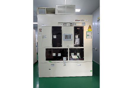
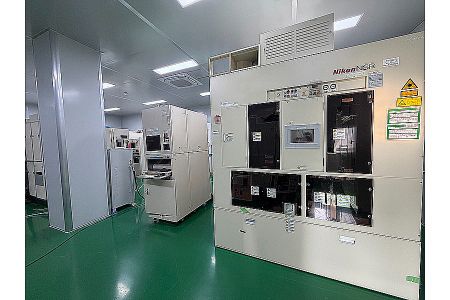
An i-line stepper is a photolithography device that uses a 365nm wavelength light source for exposure, primarily used in micron-level resolution semiconductor processes and in MEMS, power devices, and other fields. Its advantages include high stability and low cost, making it suitable for mature processes and thick photoresist applications.
The i-line stepper achieves high-precision pattern transfer by projecting a scaled-down circuit pattern from a mask onto the surface of a photoresist-coated wafer. The resolution of an i-line stepper is typically around 350nm, suitable for mature processes and micron-level structure fabrication. Due to the longer wavelength of the light source used, the i-line system exhibits excellent performance in terms of photoresist thickness and wafer warpage tolerance, making it particularly suitable for thick photoresist processes and compound semiconductor wafers with significant warpage, such as SiC and GaN. The equipment is equipped with an autofocus, multi-point leveling, and high-precision alignment system to ensure exposure quality and the accuracy of multi-layer pattern overlap. Compared to advanced deep ultraviolet lithography equipment, i-line steppers are less expensive, more stable in operation, and easier to maintain, making them suitable for low-to-medium resolution requirements and high-volume production applications. In addition, i-line steppers are also frequently used in education and R&D fields due to their lower price and lower operating threshold. Overall, i-line steppers continue to play an important role in mature manufacturing processes, and are particularly suitable for applications such as power devices, MEMS, and sensors. Choose M&R NANO TECHNOLOGY for high-quality semiconductor & optoelectronic process equipment and reliable customized manufacturing.
i-line Stepper
An i-line stepper is a photolithography device that uses a 365nm wavelength light source for exposure, primarily used in micron-level resolution semiconductor processes and in MEMS, power devices, and other fields. Its advantages include high stability and low cost, making it suitable for mature processes and thick photoresist applications.
The i-line stepper achieves high-precision pattern transfer by projecting a scaled-down circuit pattern from a mask onto the surface of a photoresist-coated wafer. The resolution of an i-line stepper is typically around 350nm, suitable for mature processes and micron-level structure fabrication. Due to the longer wavelength of the light source used, the i-line system exhibits excellent performance in terms of photoresist thickness and wafer warpage tolerance, making it particularly suitable for thick photoresist processes and compound semiconductor wafers with significant warpage, such as SiC and GaN. The equipment is equipped with an autofocus, multi-point leveling, and high-precision alignment system to ensure exposure quality and the accuracy of multi-layer pattern overlap. Compared to advanced deep ultraviolet lithography equipment, i-line steppers are less expensive, more stable in operation, and easier to maintain, making them suitable for low-to-medium resolution requirements and high-volume production applications. In addition, i-line steppers are also frequently used in education and R&D fields due to their lower price and lower operating threshold. Overall, i-line steppers continue to play an important role in mature manufacturing processes, and are particularly suitable for applications such as power devices, MEMS, and sensors.
Specifications
- Resolution: Up to 350 nm (optional)
- Numerical Aperture (NA): 0.45
- Exposure Light Source: i-line (365 nm)
- Reduction Ratio: 1:5
- Maximum Exposure Field: 22 mm × 22 mm
- Overlay Accuracy: SMO (Same-Machine Overlay Accuracy) ≤ 70 nm (optional)
- Wafer Size: Supports 2-8 inch wafers
- Wafer Thickness & Warpage: Supports various wafer thicknesses and warpages
- Backside Alignment: IR transmissive type
- Wide DOF: Extends the depth of field range
- Multipoint AF: Improves horizontal focusing
Configuration
- Exposure light source
- Projection optics and magnification
- Resolution and numerical aperture (NA)
- Exposure field size (maximum exposure field)
- Alignment system (overlay control)
Options
- Multi-point autofocus (AF)
- Wide Depth of Focus (DOF)
- Backside Alignment (IR Transmission Type)
- Supports various wafer sizes and thicknesses, and warp tolerance
- Precision wafer stage leveling/platform tire correction mechanism
Applications
- MEMS Manufacturing Process
- Sensors & Packaging
- Mature Node (>90nm) Processes in Memory
- Compound Semiconductor (SiC, GaN) Wafer Manufacturing Processes
- Educational and R&D Applications
Hot Products

i-line Stepper Professional Custom Semiconductor & Optoelectronic Process Equipment
M&R NANO TECHNOLOGY provides high-quality i-line Stepper and semiconductor & optoelectronic process equipment designed for advanced semiconductor, optoelectronic, and testing applications. Our product line includes detailed Mask Aligners, Spin Coaters, and Developers manufactured in our Taoyuan, Taiwan facility with strong automation capabilities.
We focus on delivering stable quality and precise customization through our in-house R&D and miniaturization technology. This ensures that every system meets strict process requirements while maintaining practical durability, low cost, and high efficiency for end-users.
For global buyers, M&R NANO TECHNOLOGY offers dependable manufacturing support that simplifies the sourcing process. We provide responsive communication, efficient automation integration, and consistent after-sales maintenance to help customers successfully bring their semiconductor & optoelectronic process equipment into production.